Session 4. Bit-level design of combinational systems (with logic bits)
Once here, the students have to develop their skills to solve from basic exercises to combinational circuits.
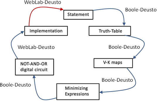
The design process of a bit-level combinational system consists on converting each representation of the digital system into another, until the digital circuit based on logic gates is reached. Thus, the first thing is to read and understand the statement of the digital system to design to determine the number of digital inputs and outputs of the system, then the truth table associated to that behaviour is written, followed by V-K map for each exit, and from all of these the corresponding simplified Boolean expressions are obtained. Lastly, the logic circuit based on logic gates NOT-AND-OR to be implemented, is obtained in the laboratory (Figure).
The process can be followed using Boole-Deusto and WebLab-Deusto. There are two key moments: the first and last one, the remaining ones are steps more or less automatic.
In the first step, the student has to obtain the truth table from a statement, and for that it has to understand it and split it case by case. The result is a truth table and will be obtained helped by the intelligence (logic) and its experience.

Lastly, the student has to test the circuit in WebLab-Deusto to decide whether this behaves as the statement requires or not. If the answer is YES, the design has concluded, but if the analysis result is NOT, then the wrong step has to be corrected, to implement back and analyse the result.